Samsung 2000 Annual Report Download - page 36
Download and view the complete annual report
Please find page 36 of the 2000 Samsung annual report below. You can navigate through the pages in the report by either clicking on the pages listed below, or by using the keyword search tool below to find specific information within the annual report.-
 1
1 -
2
-
3
-
4
-
5
-
6
-
7
-
8
-
9
-
10
-
11
-
12
-
13
-
14
-
15
-
16
-
17
-
18
-
19
-
20
-
21
-
22
-
23
-
24
-
25
-
 26
26 -
 27
27 -
 28
28 -
 29
29 -
 30
30 -
 31
31 -
 32
32 -
 33
33 -
 34
34 -
 35
35 -
 36
36 -
 37
37 -
 38
38 -
 39
39 -
 40
40 -
 41
41 -
 42
42 -
 43
43 -
 44
44 -
 45
45 -
 46
46 -
47
-
48
-
49
-
50
-
51
-
52
-
53
-
54
-
55
-
56
-
57
-
58
-
59
-
60
-
61
-
62
-
63
-
64
-
65
-
66
-
67
-
68
-
69
-
70
-
71
-
72
-
73
-
74
-
75
-
76
-
77
-
78
-
79
-
80
-
81
-
82
-
83
-
84
-
85
-
86
-
87
-
88
 |
 |

Wafers Grow Up
Our new 12-inch wafer
fabrication technology will
allow us to produce over twice
as many chips per wafer as
today’s 8-inch lines, giving us a
major competitive advantage
as the industry moves to
higher-margin 256Mb and
512Mb chips.
Cards With Smarts
Whether it’s facilitating e-
commerce, building customer
loyalty, paying for a phone call
or bus fare, or simply providing
identification, our full-range of
contact and contactless smart
cards are the perfect solution.
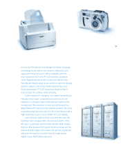
Mobile High-Definition
The next generation of
cdma2000 1x and GPRS mobile
phones are making video-on-
the-go a reality. Our new high-
resolution 720 x 240-pixel
poly-silicon reflective TFT-LCD
ensures the viewing
experience is as sharp and
clear as possible.
More Memory To Go
Leaping from 0.18-micron to
0.15-micron technology in just
a six-month period, we
boosted our NAND flash mem-
ory chip capacities from 256Mb
to 512Mb with the world’s
smallest die size to date. And
0.12-micron is just around the
corner.
36
“The networked multimedia future is going to require lots of memory. In
2000, we developed the world’s first 0.10-micron process technology for
the next generation of 4Gb DRAM chips…. This technology will soon be
dramatically increasing per-wafer yields of our 128Mb and 256Mb chips
as we lead the industry in introducing higher-capacity, higher-margin
512Mb and 1Gb chips.”
—Su-Jin Ahn, Senior Engineer, Technology Development Team