Sony 2004 Annual Report Download - page 33
Download and view the complete annual report
Please find page 33 of the 2004 Sony annual report below. You can navigate through the pages in the report by either clicking on the pages listed below, or by using the keyword search tool below to find specific information within the annual report.-
 1
1 -
2
-
3
-
4
-
5
-
6
-
7
-
8
-
9
-
10
-
11
-
12
-
13
-
14
-
15
-
16
-
17
-
18
-
19
-
20
-
21
-
22
-
 23
23 -
 24
24 -
 25
25 -
 26
26 -
 27
27 -
 28
28 -
 29
29 -
 30
30 -
 31
31 -
 32
32 -
 33
33 -
 34
34 -
 35
35 -
 36
36 -
 37
37 -
 38
38 -
 39
39 -
 40
40 -
 41
41 -
 42
42 -
 43
43 -
44
-
45
-
46
-
47
-
48
-
49
-
50
-
51
-
52
-
53
-
54
-
55
-
56
-
57
-
58
-
59
-
60
-
61
-
62
-
63
-
64
-
65
-
66
-
67
-
68
-
69
-
70
-
71
-
72
-
73
-
74
-
75
-
76
-
77
-
78
-
79
-
80
-
81
-
82
-
83
-
84
-
85
-
86
-
87
-
88
-
89
-
90
-
91
-
92
-
93
-
94
-
95
-
96
-
97
-
98
-
99
-
100
-
101
-
102
-
103
-
104
-
105
-
106
-
107
-
108
-
109
-
110
 |
 |

31
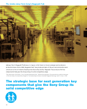
One of the world’s most advanced
semiconductor fabs
Nagasaki Fab started out as the semiconductor
production base of Sony Computer Entertain-
ment Inc. (SCE), producing advanced LSIs for
PlayStation 2 (PS2), notably the Graphics
Synthesizer (GS), a high performance graphic
rendering processor. Fab 1 began operations in
spring of 2000 and Fab 2 in spring of 2001.
Since then, Sony has continued to upgrade
both fabs with the latest production equip-
ment. The two fabs have a total of three clean
rooms. Fab 1 produces chips on 200mm wafers
using 0.18–0.15 micrometer processes (one
micrometer equals 1/1,000 of one mm). On the
upper level of Fab 2, another line processes
200mm wafers utilizing 90 nanometer (one
nanometer equals 1/1,000 of a micrometer)
technology. As of spring 2004, there were only
a few fabs in the global semiconductor indus-
try using a 90 nanometer mass-production
process, giving Nagasaki Fab recognition as
one of the world’s most advanced wafer fabs.
A vital strategic base for the Sony Group
In November 2003, the Semiconductor
Solutions Network Company (SSNC) was
established within Sony Corporation. This
gave the Sony Group an integrated frame-
work within which to implement its semi-
conductor strategy, including semiconductor
development and design. In order to further
enhance and integrate its semiconductor manu-
facturing operations, SCE’s semiconductor
production business will be merged with Sony
Semiconductor Kyushu Corporation (SCK) in
July 2004 (meaning that SCK will now be
responsible for all production operations). In
areas such as production, personnel and
technology, the two units already have a
history of extremely close cooperation. Formal
integration is expected to deepen these ties,
strengthening Sony’s semiconductor produc-
tion system and further enhancing the effi-
ciency of its operations.
Cumulative capital investments in Nagasaki
Fab through March 2004 totaled approxi-
mately ¥290 billion. The fab is now equipped
with the most advanced semiconductor pro-
cess technology in the world. Since the fiscal
year ended March 31, 2004, Nagasaki Fab
has been preparing for 300mm wafer, 65
nanometer process technology production
lines on the lower level of Fab 2. This will
enable fabrication of many sophisticated pro-
cessors that will inevitably be at the heart of
next generation digital consumer electronics
products and computer entertainment sys-
tem. Nagasaki Fab will be increasingly impor-
tant as the Sony Group’s strategic base for
semiconductor production as it establishes a
mass-production system with 65 nanometer
process technology.
Staff wearing particle-free suits called Clean Suits Electrical testing after packaging
200mm wafer in manufacturing process Surface inspection stage of the LSI production process