Sony 2004 Annual Report Download - page 35
Download and view the complete annual report
Please find page 35 of the 2004 Sony annual report below. You can navigate through the pages in the report by either clicking on the pages listed below, or by using the keyword search tool below to find specific information within the annual report.-
 1
1 -
2
-
3
-
4
-
5
-
6
-
7
-
8
-
9
-
10
-
11
-
12
-
13
-
14
-
15
-
16
-
17
-
18
-
19
-
20
-
21
-
22
-
23
-
24
-
 25
25 -
 26
26 -
 27
27 -
 28
28 -
 29
29 -
 30
30 -
 31
31 -
 32
32 -
 33
33 -
 34
34 -
 35
35 -
 36
36 -
 37
37 -
 38
38 -
 39
39 -
 40
40 -
 41
41 -
 42
42 -
 43
43 -
 44
44 -
 45
45 -
46
-
47
-
48
-
49
-
50
-
51
-
52
-
53
-
54
-
55
-
56
-
57
-
58
-
59
-
60
-
61
-
62
-
63
-
64
-
65
-
66
-
67
-
68
-
69
-
70
-
71
-
72
-
73
-
74
-
75
-
76
-
77
-
78
-
79
-
80
-
81
-
82
-
83
-
84
-
85
-
86
-
87
-
88
-
89
-
90
-
91
-
92
-
93
-
94
-
95
-
96
-
97
-
98
-
99
-
100
-
101
-
102
-
103
-
104
-
105
-
106
-
107
-
108
-
109
-
110
 |
 |
33
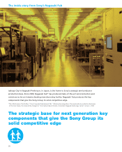
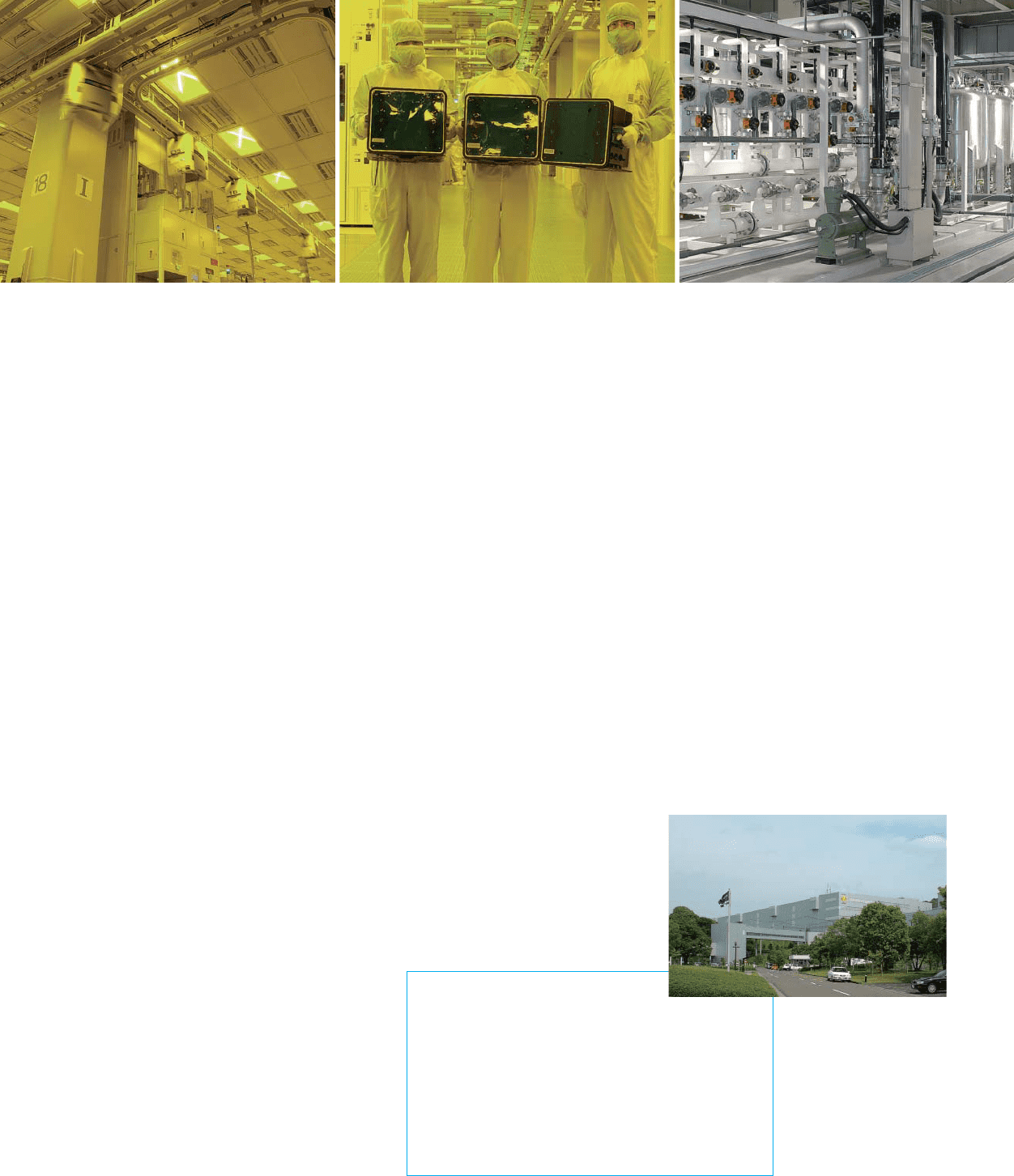
A zero-emission facility backed by
advanced energy conservation and
environmental technologies
Environmental preservation and energy conser-
vation technologies are found throughout
Nagasaki Fab, where operations adhere to
two principles: 1) coexisting in harmony with
people, that is to say, making products that
do not contain prohibited substances and
2) reducing environmental impact. Advanced
technologies and know-how in the semicon-
ductor business are applied to protect the envi-
ronment. One illustration is a zero-emission
program that has raised the facility’s recycling
rate for waste materials to 99.8%. Since wafer
fabs use large amounts of pure water and
liquid chemicals, sound facility management is
essential. At Nagasaki Fab, three different
elevations of the site are utilized for a gravity-
driven wastewater removal and treatment
system. This reduces the electricity used on
pumps by 20%. Use of the SMIF method
further reduces energy consumption.
Overview of Nagasaki Fab
Location: Isahaya City, Nagasaki Prefecture, Japan
Total site area: 99,000m2
Clean room floor area:
Fab 1—11,120m2
Fab 2—20,000m2
Wafer processing capacity per month (200mm):
Fab 1—Approx. 12,000 wafers
Fab 2—Approx. 9,000 wafers*
*This does not include the processing capacity of the fab line on the lower level
of Fab 2, which is used for producing next generation semiconductor chips.
Increasing the Sony Group’s
competitiveness
Nagasaki Fab, constructed in a short time
frame and now established as one of the
world’s most advanced semiconductor
fabrication facilities, has amassed various
technological know-how, while achieving the
highest level of productivity in the industry.
Three key factors have underpinned these
accomplishments. First is the feedback loop in
quality detection and production technology.
Second is the high degree of freedom in
process management afforded by the
adoption of SMIF. Third is taking advantage
of the fact that a large customer, that is Sony,
already exists for the production and
shipments of these components. These accom-
plishments, which represent a major com-
petitive advantage, will be indispensable
elements in the Sony Group’s design and
development of various digital consumer
electronics products and computer entertain-
ment system in the years ahead.
The automated material handling system installed
to new 300mm wafer line
FOUP holding 300mm wafers Deionized water system for ultra high-purity water