Sony 2004 Annual Report Download - page 34
Download and view the complete annual report
Please find page 34 of the 2004 Sony annual report below. You can navigate through the pages in the report by either clicking on the pages listed below, or by using the keyword search tool below to find specific information within the annual report.-
 1
1 -
2
-
3
-
4
-
5
-
6
-
7
-
8
-
9
-
10
-
11
-
12
-
13
-
14
-
15
-
16
-
17
-
18
-
19
-
20
-
21
-
22
-
23
-
 24
24 -
 25
25 -
 26
26 -
 27
27 -
 28
28 -
 29
29 -
 30
30 -
 31
31 -
 32
32 -
 33
33 -
 34
34 -
 35
35 -
 36
36 -
 37
37 -
 38
38 -
 39
39 -
 40
40 -
 41
41 -
 42
42 -
 43
43 -
 44
44 -
45
-
46
-
47
-
48
-
49
-
50
-
51
-
52
-
53
-
54
-
55
-
56
-
57
-
58
-
59
-
60
-
61
-
62
-
63
-
64
-
65
-
66
-
67
-
68
-
69
-
70
-
71
-
72
-
73
-
74
-
75
-
76
-
77
-
78
-
79
-
80
-
81
-
82
-
83
-
84
-
85
-
86
-
87
-
88
-
89
-
90
-
91
-
92
-
93
-
94
-
95
-
96
-
97
-
98
-
99
-
100
-
101
-
102
-
103
-
104
-
105
-
106
-
107
-
108
-
109
-
110
 |
 |

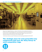
32
Setting the industry standard for time to
commission a new fab
Speed was essential when Fab 1 was built.
Fab 1 had to be able to supply a large volume
of semiconductors for PS2, which was sched-
uled to go on sale in March 2000, meaning
that SCE needed to set a new standard for
speed in commissioning a new fab. Construc-
tion began in spring 1999. Only five and a half
months was needed to complete the Fab 1
clean room, while production of prototypes
began in the ninth month following the instal-
lation of equipment. The construction period
was about half of the industry norm at that
time, thereby setting a new industry standard.
Productivity well above the
industry standard
Early adoption of the new Standard of
Mechanical Interface (SMIF) production
system is one reason Nagasaki Fab is the
leader in productivity in the fabrication of
advanced semiconductors. Another is the
existence of PS2, a product sold in enormous
volumes worldwide.
When fabricating semiconductors, even the
tiniest speck of airborne dust can ruin a chip.
That is why wafer fabs typically place manufac-
turing equipment in a class 1 (one dust particle
or less per cubic foot) clean room, one of the
highest standards for these types of facilities.
The SMIF method, on the other hand, does not
place the entire production line into a clean
room. Instead, only the insides of production
machines and the SMIF-Pod, where wafers
are stored, need to be raised to class 1 level.
Thanks to this technology, Sony gained much
more freedom in the layout of production
machinery and management of each process.
The result is improvements in capacity utiliza-
tion and overall productivity.
Cumulative production shipments of PS2
surpassed 70 million units only four years
after its introduction, and high shipment
volumes continue. From the beginning,
Nagasaki Fab produced the GS, one of the
core semiconductor components for PS2 and
a key factor in its performance. The enormous
popularity of PS2 forced the fab to make
constant improvements in productivity in
order to ensure a large and reliable supply of
chips. GS is an LSI with embedded DRAM,
making it more complex than ordinary logic
LSIs. Manufacturing GS and other specialized
chips in large quantities is one of the greatest
strengths of Nagasaki Fab. This skill has
enabled the fab to raise productivity to one of
the highest levels through its focus on
improvements in production processes.
Central to raising productivity has been an
unrivaled quality evaluation and analysis
system, permitting the detailed monitoring of
quality as each process is under way. This
system improves the ability to detect and
instantly respond to abnormalities, raising
both quality level and productivity.
An optimal production strategy based on
process technologies
At Nagasaki Fab, the best possible production
strategies are formulated and executed based
on the process technologies used on each
line. Currently, the 0.18–0.15 micrometer line
at Fab 1 produces LSIs for PS2; Wega Engine,
an image quality enhancing signal processor
for Sony televisions; video cameras and other
AV products. In the near future, this line will
be used to manufacture CMOS image sen-
sors, a component for which demand is likely
to rise, especially for use in mobile products.
The 90 nanometer line on the upper level of
Fab 2 produces a highly sophisticated chip that
integrates GS and EmotionEngine (EE), a 128-
bit CPU for PS2 into a single chip. This chip,
which has 53.5 million transistors, is used in
PSX, a DVD recorder. Benefits of this chip
include reductions in both power consumption
and production costs. This line is planned to
be used for the production of the CPU for
PlayStation Portable (PSP), a handheld video
game system that is expected to go on sale
during the fiscal year ending March 31, 2005.
On the lower level of Fab 2, the 65 nano-
meter process line employs the FOUP (Front
Opening Unified Pod) method, a technique
that takes SMIF to a higher level. Additionally,
this facility is moving toward complete auto-
mation by integrating the AMHS (Automated
Material Handling System) and MES (Manu-
facturing Execution System). Armed with
these cutting-edge processes, this fab plans
to produce some of the most sophisticated
microprocessors for use in next generation
digital consumer electronics products and
computer entertainment system.
SMIF technology achieves local clean areas A material handling box used for SMIF technology State of the art equipment for ultra-fine processing