Sony 2012 Annual Report Download - page 28
Download and view the complete annual report
Please find page 28 of the 2012 Sony annual report below. You can navigate through the pages in the report by either clicking on the pages listed below, or by using the keyword search tool below to find specific information within the annual report.-
 1
1 -
2
-
3
-
4
-
5
-
6
-
7
-
8
-
9
-
10
-
11
-
12
-
13
-
14
-
15
-
16
-
17
-
 18
18 -
 19
19 -
 20
20 -
 21
21 -
 22
22 -
 23
23 -
 24
24 -
 25
25 -
 26
26 -
 27
27 -
 28
28 -
 29
29 -
 30
30 -
 31
31 -
 32
32 -
 33
33 -
 34
34 -
 35
35 -
 36
36 -
 37
37 -
 38
38 -
39
-
40
-
41
-
42
-
43
-
44
-
45
-
46
-
47
-
48
-
49
-
50
-
51
-
52
-
53
-
54
-
55
-
56
-
57
-
58
-
59
-
60
-
61
-
62
-
63
-
64
-
65
-
66
-
67
-
68
-
69
-
70
-
71
-
72
 |
 |

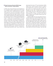
High-image-quality
pixel technology
Commercialization of CCD (1980)
On-chip column parallel
A/D conversion
Commercialization of
ExmorTM (2007)
Back-illuminated structure
Commercialization of
Exmor RTM (2009)
Stacked structure
Commercialization of stacked
CMOS image sensor (2012)
Ever-increasing wealth
of innovative technology
10 15 10 200 200 200 2010 2011 2012
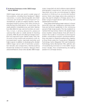
Newly Developed Stacked CMOS Image
Sensor Introduces “Super Reality”
In 1978, Sony announced that it had developed a
0.11 megapixel charge-coupled device (CCD) image
sensor. Since then, underpinned by its superior
semiconductor process technologies, Sony has
ceaselessly pursued the development of image
sensors that provide both high resolution and ease
of use. While maintaining the leading market share
for CCD image sensors, in 2007 Sony developed the
ExmorTM image sensor by capitalizing on the low
power consumption and high speed of comple-
mentary metal oxide semiconductor (CMOS) tech-
nology, as well as on high-image-quality pixel
technology nurtured through development of the
CCD. Using Sony’s proprietary on-chip column par-
allel analog-digital (A/D) conversion and dual noise
reduction technologies, ExmorTM achieved in-
creased speed and lower noise. Then in 2008, Sony
developed the Exmor RTM back-illuminated CMOS
image sensor, which enables cameras to capture
clear images even in scenes lit only by candle. Im-
age sensors are imaging elements that may be
thought of as the “eyes” of digital cameras. Sony’s
technologies have thus supported the advance-
ment of image sensors, contributing greatly to
enhancements in image resolution and camera
speed, enabling Sony to build technical and com-
petitive advantages.
In January 2012, Sony announced that it had suc-
cessfully developed a stacked CMOS image sensor.
In place of the supporting substrate used in con-
ventional back-illuminated CMOS image sensors,
this groundbreaking new image sensor layers the
pixel section containing formations of back-illumi-
nated structure pixels onto chips containing the cir-
cuit section for signal processing. Fabrication of
this structure requires state-of-the-art precision in
semiconductor process technology. Sony was able
26