Sony 2012 Annual Report Download - page 29
Download and view the complete annual report
Please find page 29 of the 2012 Sony annual report below. You can navigate through the pages in the report by either clicking on the pages listed below, or by using the keyword search tool below to find specific information within the annual report.-
 1
1 -
2
-
3
-
4
-
5
-
6
-
7
-
8
-
9
-
10
-
11
-
12
-
13
-
14
-
15
-
16
-
17
-
18
-
 19
19 -
 20
20 -
 21
21 -
 22
22 -
 23
23 -
 24
24 -
 25
25 -
 26
26 -
 27
27 -
 28
28 -
 29
29 -
 30
30 -
 31
31 -
 32
32 -
 33
33 -
 34
34 -
 35
35 -
 36
36 -
 37
37 -
 38
38 -
 39
39 -
40
-
41
-
42
-
43
-
44
-
45
-
46
-
47
-
48
-
49
-
50
-
51
-
52
-
53
-
54
-
55
-
56
-
57
-
58
-
59
-
60
-
61
-
62
-
63
-
64
-
65
-
66
-
67
-
68
-
69
-
70
-
71
-
72
 |
 |

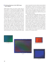
to make this breakthrough thanks to its unique
strengths in high-resolution technologies, know-
how cultivated in the CCD field and cutting-edge
metal oxide semiconductor (MOS) technology. This
success in developing the stacked structure opens
up room for large-scale circuits to be built in,
achieving further enhancement in image quality,
superior functionality and a more compact size for
digital cameras and mobile devices. The new struc-
ture is positioned to become the next generation
of back-illuminated CMOS image sensors. Today,
Sony is taking steps to fur ther enhance CMOS
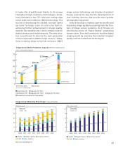
Image Sensor Market by Main Usage
(FY08–FY15)
(100 million units)
20
16
12
8
4
0
Quantity
CAGR +11%
200 2010 2011 2012 2013 201 2015 201
.2
10.5
12.0
1. 15. 1. 1. 1.
. . . 12.5
13. 1. 15.3 1.3
Cellular Digital Camera Security Camera
D-SLR Video Camera
Image Sensor Market by Main Usage
(FY08–FY15)
(10 billion yen)
75
60
45
30
15
0
Amount
CAGR +8%
Cellular Digital Camera Security Camera
D-SLR Video Camera
200 2010 2011 2012 2013 201 2015 201
1. 1.1 2.5 .0
5.0
0.2
5. .3
15.2 1. 15.3 1.2 22.1 25. 2. 31.5
11.3 . .0 . .2 . .0 .2
. 10.0 11.5
12.2
1.0
20.0
20. 22.0
December 2010
As of press release date
March 2012
5
0
5
30
15
2 times
1. times
0
2011
200 300mm wafer
300mm wafer
200mm wafer
2 s/m
0 s/m
s/m
Kagoshima TEC Nagasaki TEC Fab1
Kumamoto TEC Nagasaki TEC Fab3 Nagasaki TEC Fab2
Production contracted to third parties
December 2010
As of press release date
March 2012
5
0
5
30
15
2 times
1. times
0
2011
200 300mm wafer
300mm wafer
200mm wafer
2 s/m
0 s/m
s/m
Kagoshima TEC Nagasaki TEC Fab1
Kumamoto TEC Nagasaki TEC Fab3 Nagasaki TEC Fab2
Production contracted to third parties
image sensor technology and broaden its product
lineup, paving the way for the development of
user-friendly cameras that provide even greater
photography enjoyment.
Sony technology is making cameras smaller and
improving image quality by pushing back the fron-
tiers of image sensor evolution. As it focuses on
introducing an era of “Super Reality” surpassing
human vision, Sony will continue to lead the digital
imaging world by ensuring the industry’s highest
quality and most advanced technologies.
27
Image Sensor Market by Main Usage * Sony estimates
Image Sensor Wafer Production Capacity (300mm wafer basis)
Note: Years ended March 31.
(unit: 1,000 wafers/month)