Sony 2011 Annual Report Download - page 27
Download and view the complete annual report
Please find page 27 of the 2011 Sony annual report below. You can navigate through the pages in the report by either clicking on the pages listed below, or by using the keyword search tool below to find specific information within the annual report.
25
Investment in the image sensor business
On September 1, 2010, Sony announced that it planned to
invest approximately 40 billion yen in Sony Semiconductor
Kyushu Corporation’s Kumamoto Technology Center
(Kumamoto TEC) to increase production capacity for “Exmor”
and “Exmor R” CMOS image sensors. Execution of this
additional investment would be spread between the second
half of fiscal year 2010, ended March 31, 2011, and fiscal year
2011, ending March 31, 2012.
Furthermore, on December 27, 2010, Sony announced plans
to invest approximately 100 billion yen in Sony Semiconductor
Kyushu Corporation’s Nagasaki Technology Center (Nagasaki
TEC) during fiscal year 2011, ending March 31, 2012, to
increase the production capacity for CMOS image sensors. This
investment plan includes (i) semiconductor fabrication equipment
acquired on April 1, 2011, based on definitive agreements
between Sony and Toshiba Corporation announced on
February 28, 2011; (ii) refurbishment of a part of these
semiconductor fabrication facilities into new wafer lines capable
of manufacturing CMOS image sensors; and (iii) refurbishment
of and equipment for part of the production facilities at Nagasaki
TEC’s Building 3 for wafer processing for the purpose of
differentiating Sony’s CMOS image sensors using proprietary
technologies. Within this investment program, principally in
relation to item (iii) above, Sony is utilizing subsidies provided
under the Japanese Government’s fiscal year 2010 “Project to
promote plant construction in industries that create low-carbon-
type employment” administered by the Ministry of Economy,
Trade and Industry.*
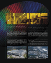
Sony Semiconductor Kyushu Corporation’s Kumamoto Technology Center Sony Semiconductor Kyushu Corporation’s Nagasaki Technology Center
* Through Sony Semiconductor Kyushu’s investments of approximately 40 billion
yen in Kumamoto TEC and approximately 100 billion yen in Nagasaki TEC as
outlined above, Sony plans to increase its total manufacturing capacity for CCD
and CMOS image sensors from its current level of approximately 25,000 units
per month to approximately 50,000 units per month (calculation for 300mm
wafers, as of December 27, 2010) by the end of March 2012.


